Canon Introduces a New Lithography System with Large Exposure Field at a High Resolution for Producing Full-frame CMOS Sensors, XR devices and Others
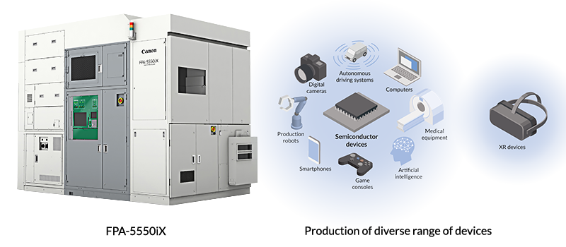
SINGAPORE, March 13, 2023 — Canon announced today that the company will release the FPA-5550iX i-line stepper1 semiconductor lithography system for front-end processes that realizes a large exposure field of 50 x 50 mm and a high resolution of 0.5 micrometers2.
The new system features a large exposure field of 50 x 50 mm and a high resolution of 0.5 micrometers making possible single exposure of a large field with the high resolution required to produce full-frame CMOS sensors and other devices in which higher precision is advancing. The new system is also capable of manufacturing small displays for such devices as head-mounted displays. It also enables the high-resolution single exposure required for manufacturing high-contrast micro-OLED panels3 with wide viewing angles, which are expected to grow as displays for cutting-edge XR devices. In addition to semiconductor devices, the new FPA-5550iX can also manufacture displays for cutting-edge XR devices, thus supporting the manufacture of a wide range of devices.
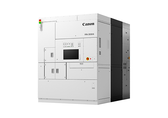
The FPA-5550iX utilizes the same projection lens used by its predecessor model, the FPA-5510iX (released in September 2015) which enables a high resolution of 0.5 μm. Thanks to a wide exposure field of 50 x 50 mm, the system can perform high-resolution single exposure for full-frame CMOS sensors, next-generation displays for XR devices and more. What’s more, manufacturing processes have been refined to ensure high-quality, stable production of projection lenses, many of which are used in the system, to meet the strong demand expected for semiconductor lithography systems.
In addition, a new alignment scope that can read wider variety of alignment marks4 has expanded the range of processes in which FPA-5550iX can be used. In addition to the "bright-field detection" function for measuring direct light, a new "dark-field detection" function has been added to the alignment scope, enabling the measuring of scattered and diffracted light, thus allowing users to select a wide range of measurement methods. Low-noise measurement has been made possible by expanding the range of usable wavelengths while also employing an area sensor for multi-pixel measurement. Thanks to these advancements, the system can detect and measure low-contrast alignment marks. What’s more, the system can optionally select an infrared wavelength that can pass through silicon, enabling users to measure the alignment on the back of the wafer, which is a requirement for the manufacture of back-illuminated sensors. The flexibility of alignment mark measurement thus allows the system to be utilized in a variety of processes.
When combined with Canon’s Lithography Plus solution platform (released in September 2022), the FPA-5550iX, provides operators with the ability to monitor the condition of the lithography system, as well as perform analyses, helping them maintain appropriate quality control and higher utilization rates.
About Canon Singapore Pte. Ltd.
Canon is a global leader in photographic and digital imaging solutions. Canon Singapore Pte. Ltd. is the headquarters for South & Southeast Asia driving sales, marketing and service strategies. Besides handling the domestic market, the company covers 22 other countries and regions including subsidiaries in India, Malaysia, Thailand and Vietnam. The parent company Canon Inc. has a global network of more than 300 companies and employs about 180,000 people worldwide. Canon is guided by its kyosei philosophy that focuses on living and working together for the common good.
More information is available at https://asia.canon.
1 A semiconductor lithography system that utilizes a 365 nm wavelength mercury lamp as the light source. 1 nm (nanometer) is 1 billionth of a meter.
2 1 micrometer = 1/1,000,000 meter.
3 A production method for ultra-high resolution displays, made with silicon wafers featuring image quality characteristic to OLED.
4 Marks placed on silicon wafers to secure accurate circuit pattern overlay.